PCB design guidelines for fabrication
Most fabrication delays start with the data, not the design. These rules cover what to send, how to set up each layer and the questions to answer up front, so your boards go straight from engineering review into production.
- Gerber format we work from
- RS-274X
- Drill size step: merge sizes closer than this
- 0.05 mm
- Smallest legend text that stays readable
- 1.00 mm
- Largest finished via a mask fill closes
- 0.25 mm
What to send
A complete fabrication package is a set of Gerber files in extended RS-274X format plus an Excellon drill file (format 1 or 2) with the tool list embedded. Include every layer the board needs:
- All copper layers, outer and inner
- Solder mask and legend (silkscreen) for each side
- The board outline or a mechanical layer with dimensions
- Solder paste layers, if we are also making a stencil or assembling
- Any special layers: carbon ink, peel-off mask, via fill
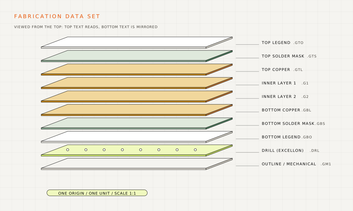
RS-274D is an obsolete format. If you have no choice but to use it, send the aperture list with it so every flash and draw can be reproduced. Native CAD files, office documents and parts lists are not needed to build a bare board, although a PDF drawing helps when the outline or build-up is unusual.
Before you release the files
- Open the exported Gerber and drill files in a viewer and check them against the design
- Name each file so its layer is obvious, or add a readme that maps files to layers
- Export at full scale (1:1) with the same units and resolution in Gerber and drill files
- Use the same origin for every layer, ideally zero offset
- Keep the view from the top: top-side text reads correctly and bottom-side text appears mirrored
Common data faults
- Very long or cryptic file names
- Apertures or drill tools with a size of zero
- Converting between mm and inch on export, which introduces rounding errors
- Mirroring or rotating individual layers
- Instructions that live only in an email instead of in the data or the readme
Drill data
- Holes must not overlap. Overlapping hits break drill bits and leave debris that can cause voids in plated barrels.
- Draw slots as slots (routed or as a slot command), never as a row of overlapping holes.
- Drills come in 0.05 mm (2 mil) steps, so merge hole sizes that are within 0.05 mm of each other.
- Send plated (PTH) and non-plated (NPTH) holes as separate files. If that is not possible, use separate tools and mark which are which.
- Where an NPTH sits on the board edge, draw it as part of the outline rather than as a hole crossing the contour.
- Call out plated holes on the board edge, such as castellations, on the mechanical layer.
Copper layers
- Output pads as flashes. Pads built from many small draws are hard to inspect and edit.
- Build planes and large areas from polygons or contours (region fills in RS-274X), never painted with strokes.
- Put the board outline on every copper layer as well as on the mechanical layer, so the layers can be aligned if an offset appears.
- Remove unconnected copper pads from NPTH holes.
- Keep copper back from the board edge by at least the clearances in the rigid PCB capabilities. If copper must reach the edge, or the edge must be plated, say so on the mechanical layer.
- Label every layer with right-reading text as seen from the top, and give inner layers a number (1 for top, 2 for the first inner layer and so on) so the order cannot be mistaken.
- Fill planes with solid copper rather than a hatch pattern.
Narrow copper features cause most etching faults. Where a plane flows between isolated pads, leave at least 0.20 mm (8 mil) between the pads so no thin sliver of copper is left to lift and short. Avoid peelable fragments and the spacing errors that arise between parts of the same net.
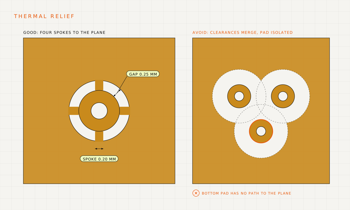
Define every thermal relief so it meets the annular ring, spoke width and gap limits. A gap of 0.25 mm (10 mil) with 0.20 mm (8 mil) spokes is a sound starting point. Check that neighbouring clearances do not overlap and cut a pad off from the plane completely.
Balanced construction
A multilayer board bows and twists when its two halves differ. Keep the number of copper layers, their copper weights and the positions of planes mirrored about the centre of the stackup. Where a layer count is odd, adding a dummy layer is usually cheaper than fighting warp.
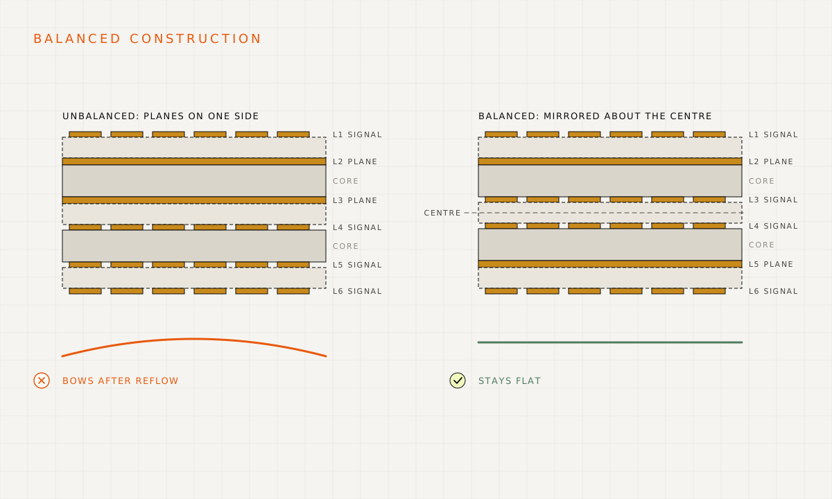
Large empty areas on inner layers cause another problem. During lamination resin and trapped air cannot flow evenly, which leaves micro-voids or starts delamination. Add copper balancing (thieving) or venting patterns to sparse inner layers so pressure spreads evenly.
Annular rings, isolation and edge clearance
Three faults account for most engineering queries on copper layers:
- Inner-layer rings that are too small break out when the drill wanders, leaving an open or a weak via. Meet the inner ring minimum in the capability tables.
- Outer-layer rings that are too small shrink the solderable land and also risk breakout.
- Isolation that is too tight for the finished copper weight leads to over-etching, shorts or impedance errors. Track and gap minimums grow with copper thickness, so design to the finished weight, not the starting foil.
- Pads and tracks too close to a routed or scored edge are damaged during profiling, exposing copper that then oxidises.
Solder mask
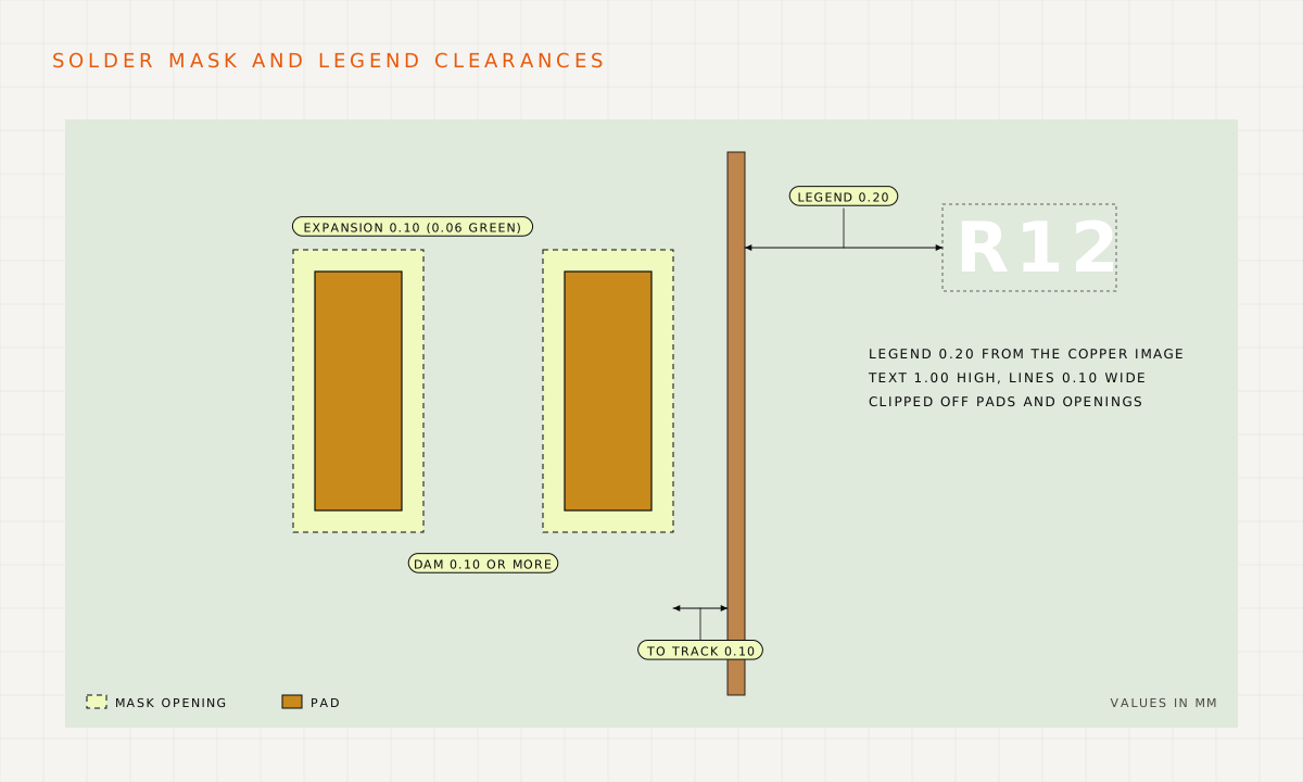
- Give each pad a mask opening 0.10 mm (4 mil) larger than the pad on every side to absorb registration error. Green and blue mask can go down to 0.06 mm when space is tight.
- Keep mask dams (the strip of mask between two openings) at 0.10 mm or more. Below that the dam may lift. Other mask colours need larger openings and wider dams than green.
- Keep 0.10 mm between a mask opening and any neighbouring track, or the track will be exposed and may short during soldering.
Legend (silkscreen)
- Use text at least 1.00 mm (40 mil) high. Smaller characters blur once printed.
- Draw legend lines 0.10 mm (4 mil) wide or wider and delete anything thinner.
- Clip legend where it would print on a pad or on a mask opening, so ink never reaches a solderable surface.
- Leave 0.20 mm (8 mil) between legend and the copper image to avoid clipped characters.
| Legend to | Clearance |
|---|---|
| Routed board edge | 0.25 mm |
| Scored (V-cut) board edge | 0.45 mm |
| Exposed copper | 0.10 mm |
| Holes and cut-outs | 0.10 mm |
For assembled boards, also keep legend clear of component bodies, especially around fine-pitch parts where reference designators often end up under the package.
Mechanical layer
The mechanical layer is the drawing the fabricator profiles the board from. As a minimum it holds the exact board outline and the position and size of every internal cut-out and slot, ideally dimensioned in mm or inch. The centre of the outline stroke is taken as the board edge, whatever its line width. Add the following as needed:
- A reference hole with its X and Y position from the outline, which matters most when NPTH holes have no pads
- A drill map using a different symbol for each size
- Which holes and slots are plated and which are not
- A layer sequence or build-up drawing listing copper, mask, legend and any special layers, top to bottom, with the matching file names
- The array drawing, if boards are to be delivered in a panel for assembly
A keep-out layer is not a substitute. Keep-out shapes tell the layout tool where copper and parts may not go; they are design rules, not fabrication instructions, and we do not profile boards from them.
Carbon, peel-off mask and via fill
Each of these needs its own Gerber layer with the board outline included, a file name that says which side it belongs to, and an entry in the build-up on the mechanical layer.
| Feature | Rule |
|---|---|
| Carbon line width | 0.30 mm (12 mil) minimum |
| Carbon to carbon spacing | 0.25 mm (10 mil) minimum |
| Carbon pad | 0.15 mm (6 mil) larger than the copper pad |
| Mask opening | 0.15 mm larger than the copper pad, the same size as the carbon pad |
Peel-off mask is normally printed on one side only, usually the bottom. Join small peel-off areas into larger ones wherever you can; scattered islands are slow to strip after soldering.
| Feature | Rule |
|---|---|
| Width of any peel-off element | 0.50 mm (20 mil) minimum |
| Largest hole it can cover (finished size) | 6.00 mm |
| Overlap onto the copper pattern | 0.254 mm (10 mil) minimum |
| Clearance to free copper | 0.254 mm (10 mil) minimum |
| Distance from the board outline | 0.50 mm (20 mil) minimum |
| Position tolerance | ±0.30 mm (12 mil) |
Via fill is the only way to guarantee a closed via. It covers the via pad and hole with a second coat of non-conductive solder mask and closes holes up to 0.25 mm (10 mil) finished size, which corresponds to a drill of about 0.35 mm. Supply a Gerber containing only the via pads to be filled, plus the outline, and say which side it is applied from. Fill is usually applied from one side.
The readme file
A short readme saves a round of questions. List each file and what it contains, the drill and PTH/NPTH details, the format details if you used RS-274D, and any special requirement. Then answer the decisions we would otherwise have to ask about:
- May non-functional pads on inner layers be removed?
- May we add copper thieving to even out plating?
- Are there areas where a logo or date code must not go?
- Should teardrops be added where tracks meet pads?
- Where an NPTH passes through copper, is a clearance ring (void rim) around it acceptable?
- If there is no room for a mask dam between fine-pitch pads, is one opening across the row (gang relief) acceptable?
- If tolerances are missing, may we use ±0.075 mm on holes, ±10% on thickness and ±0.25 mm on the outline?
Countersunk holes
A countersink is a conical recess at the top of a hole so a flat-head screw sits flush with the board surface, leaving nothing proud to foul parts or a mating assembly. Mark each countersunk hole in the drill data and give its top diameter, included angle and the side it is cut from in a note on the mechanical drawing, ideally with a small section sketch.
Ready when your files are
Send your design for a quote
Upload your Gerber, drill and assembly files with the quantities you need. Our engineers check them against these guidelines and come back with a price, a schedule and any questions.