What our assembly lines handle as standard: the technologies, the smallest and largest parts, board sizes and thicknesses, the part packaging we accept and how every build is inspected. Values are in millimetres unless stated.
FR-4, RF laminates and metal-core boards. Ask us about flexible circuits.
Board shapes
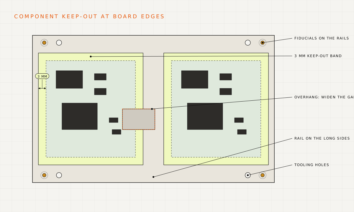
Rectangular, round and irregular. Non-rectangular boards are assembled in an array with rails on the two longer parallel sides.
Components
Parts we place
Category
Examples
Passives
Down to 01005, with 0201 and 0402 routinely placed
Fine-pitch leaded and leadless
QFN, QFP
Small outline and array packages
SOIC, PLCC, TSOP, BGA, CSP, CCGA
Power and other parts
DPAK, aluminium electrolytic and tantalum capacitors, through-hole parts
Largest part
56 x 56 x 15 mm
Smallest BGA pad
0.20
Vias in solder pads can be accepted where the design allows it. Some solder flows into an open via, so the fillet is less visible; if that is acceptable to your quality standard we can build it. Open vias in BGA pads are not accepted.
BGA and QFN pad spacing
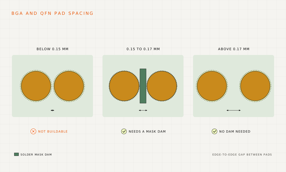
The edge-to-edge gap between neighbouring BGA or QFN pads decides whether a solder mask dam can separate them:
Pad edge-to-edge clearance
Clearance between pads
Result
More than 0.17
Buildable without a mask dam
0.15 to 0.17
Buildable only with a mask dam between the pads
Less than 0.15
Not buildable; widen the gap
Pad spacing thresholds for BGA and QFN parts.
Board size and thickness
Largest board by component pitch and thickness
Condition
Largest board (L x W)
Component pitch above 0.5
430 x 585, with a printable area of 430 x 460
Component pitch of 0.5
250 x 250
Component pitch below 0.5
200 x 200; a mask dam between pads is preferred
Board thickness 0.80 to 3.20
430 x 585, with a printable area of 430 x 460
Board thickness 0.40 to 0.80
200 x 200
Board thickness range
0.40 minimum, 3.20 maximum
Keep components 3 mm from board edges. Small passives with only a few pads near the edge can sit closer.
Component to board edge
Item
Standard capability
Component to board edge
3.00. Closer is accepted for passive parts when fewer than 6 pads face the edge.
Customer-supplied parts
Part packaging we accept
Format
Condition
Reels
Preferred
Cut tape
Continuous strips at least 300 mm (12 in) long
Tubes and trays
Accepted
Loose parts
Accepted for through-hole parts
Files and inspection
Files and checks
Item
Standard capability
BOM
.xlsx, .xls or .csv
Board data
Gerber RS-274X
Placement data
Centroid (XY or pick-and-place) file
Inspection
Visual inspection, automated optical inspection (AOI) and X-ray for hidden joints such as BGAs and QFNs
Ready when your files are
Send your design for a quote
Upload your Gerber, drill and assembly files with the quantities you need. Our engineers check them against these guidelines and come back with a price, a schedule and any questions.