PCB assembly design guidelines
An assembly quote and build depend on two files and a footprint library that matches the parts. These guidelines cover the data we need, the design choices that keep assembly simple and the board sizes our lines handle comfortably.
- Keep parts this far from a board or panel edge
- 3 mm
- Smallest passive package placed
- 01005
- Largest component body soldered
- 56 x 56 x 15 mm
- Thickest board assembled
- 3.2 mm
Assembly data
Every assembly order rests on two files, supplied with the Gerber set:
- Bill of materials (BOM): one line per part with the manufacturer part number (MPN), a description, the reference designators that use it and the quantity per board or per array. A distributor part number is a useful extra.
- Placement file (centroid, pick-and-place or XY file): for each reference designator, its X and Y position, its rotation and the side it sits on.
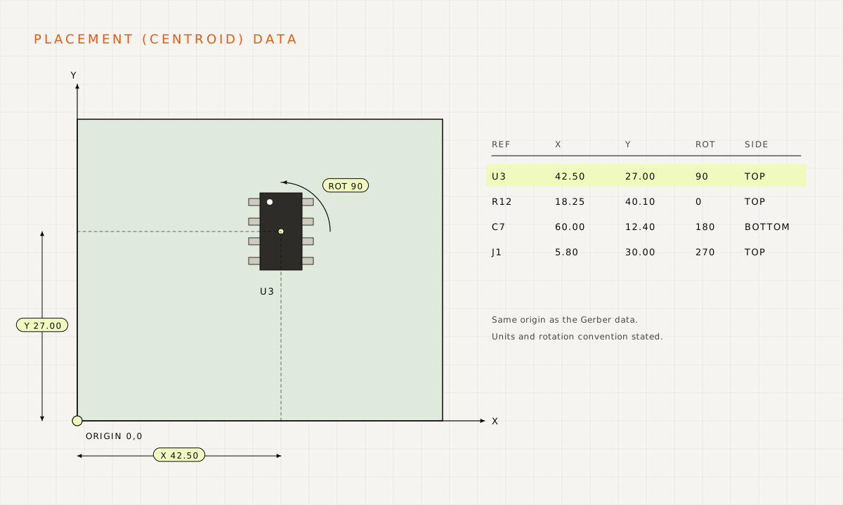
We accept the BOM as .xlsx, .xls or .csv, Gerber data in RS-274X and placement data as an XY or pick-and-place export. The origin of the placement file must match the origin of the Gerber data.
Assembly technologies
| Technology | How it is soldered | Design note |
|---|---|---|
| Surface mount (SMT) | Paste is printed through a stencil, parts are placed by machine and the board is reflowed in an oven. | Keep all SMT parts on one side when you can; a second side adds a print, a placement pass and a reflow. |
| Through-hole (THT) | Leads pass through plated holes and are soldered by wave, selective wave, hand or pin-in-paste reflow. | Plated holes pull solder up the barrel for a strong joint. Put all through-hole parts on one side to save handling. |
| Mixed technology | SMT reflow first, then through-hole soldering. | Common for boards with power devices and connectors alongside fine-pitch SMT. |
Pin-in-paste prints solder paste over and into the through-holes, so the through-hole parts reflow with the SMT parts and skip a separate soldering step. It works best with parts that can survive the reflow profile and holes sized to hold enough paste.
Footprints
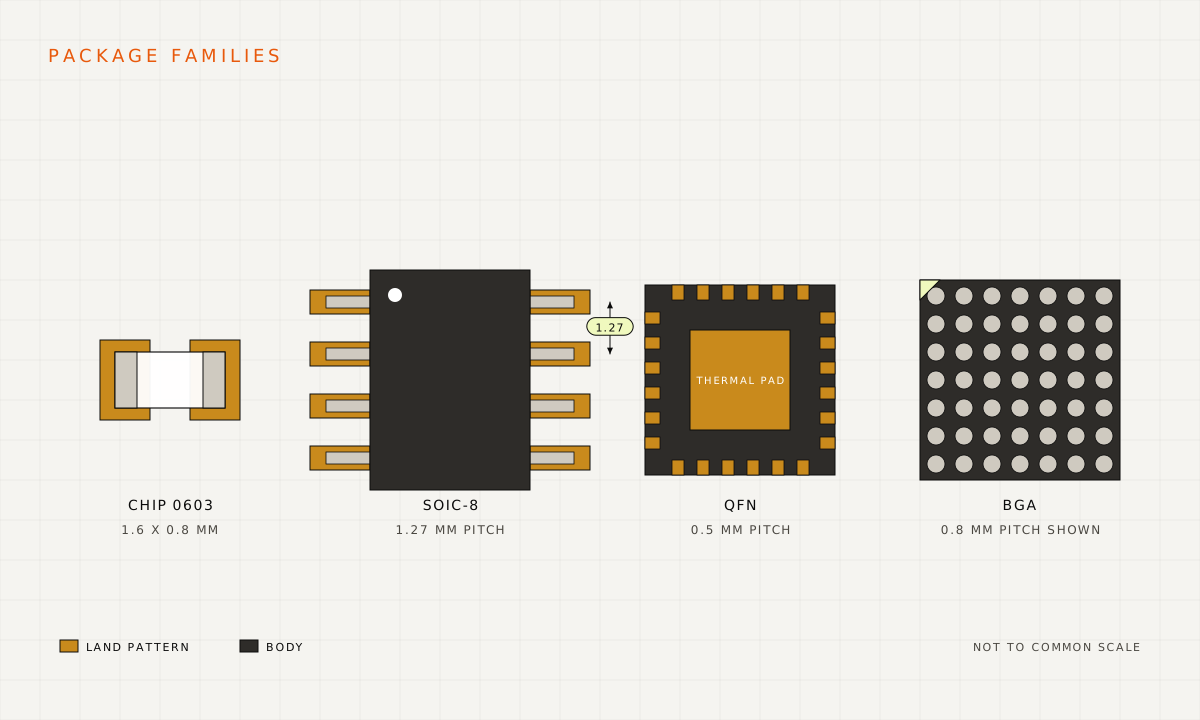
- Build footprints from the manufacturer’s datasheet, and check that pads, mask and paste line up on every layer.
- Where the recommended hole size for a through-hole lead cannot be used, make the finished hole at least 0.15 mm larger than the lead.
- Between fine-pitch pads, leave a mask web of 0.08 mm or more with green mask (opening 0.06 mm per side), or 0.12 mm with other colours (opening 0.10 mm). Keep it as small as needed, but enough to stop bridging.
- Give both pads of a two-terminal part the same size and similar copper connection. Uneven heating makes one end reflow first and stand the part on end (tombstoning).
Paste layers
- Supply paste layers at 1:1 with the copper pads. Our engineers apply aperture reductions and window-pane patterns for large pads when the stencil is made.
- Include the fiducial marks on the paste layers as well as on copper, so the stencil can be aligned to the board.
- Leave paste off pads that must not be soldered, such as test points and pads for parts marked do-not-populate.
BOM checks
- Every line has an MPN and a quantity for one board or one array.
- Every reference designator in the BOM appears in the placement file and on the board, and the descriptions match.
- Parts that are readily available keep lead times short; flag any part you know is scarce and list approved alternatives.
- When a part changes between revisions, change its part number too, so old and new versions are never mixed.
- Mark do-not-populate (DNP) parts clearly instead of deleting them from the BOM.
Component placement
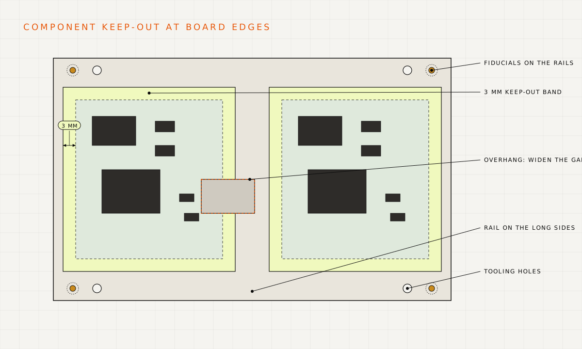
- Keep components away from board edges. Handling, rails and depaneling can damage parts that sit too close.
- Leave room between parts for the placement nozzle, for inspection and for rework. Crowded boards are slower to place and harder to test.
- For wave soldering, orient parts so all leads of a part reach the wave together, and do not put tall parts upstream of small ones where they shadow the joints.
- Spread out parts that run hot and give them airflow, rather than grouping them.
- Avoid placing very large or unusually shaped parts right next to small SMT parts; they disturb paste printing and heating.
- Place connectors where cables can be plugged in and out during assembly and test, with clearance to neighbouring boards and enclosures.
Board size and shape
Boards in the sizes below run through our lines without special fixtures. Anything outside them can still be built, often by panelising, so treat these as the comfortable range rather than hard limits; the absolute limits are on the assembly capabilities page.
| Item | Preferred range |
|---|---|
| Smallest board handled on its own | 90 x 50 mm. Smaller boards are panelised. |
| Largest board, standard parts | 500 x 300 mm |
| Largest board with parts at 0.5 mm pitch or finer (BGA, QFP, QFN) | 150 x 150 mm |
| Thin boards, 0.5 to 1.0 mm | Up to 150 x 150 mm. Agree panel details with us for anything thinner. |
| Maximum board thickness | 3.2 mm |
| Shapes | Rectangular, round or irregular. Anything not rectangular is assembled in an array with rails on at least the two longer sides. |
Edge clearance and arrays
Keep at least 3 mm between active components and the edges of every board and of the panel. If a connector or other part must overhang the board edge, deliver the boards in an array and leave extra space between neighbouring boards so the overhang clears. Assembling in an array is also usually cheaper, because parts are placed while the boards are still joined.
Ready when your files are
Send your design for a quote
Upload your Gerber, drill and assembly files with the quantities you need. Our engineers check them against these guidelines and come back with a price, a schedule and any questions.