Rigid PCB capabilities

The limits we build rigid boards to as standard, from layer count and copper weight to drill sizes, finishes and tolerances. All values are in millimetres unless stated. Design inside them and your board goes through normal production.

Maximum layers
24
Finest track and gap (0.5 oz outer)
0.09 mm
Smallest finished via
0.10 mm
Largest FR-4 board
430 x 585 mm

Board size, layers and copper

Layers and thickness
ItemStandard capability
Maximum layers24
Maximum finished thickness3.20 mm
Minimum finished thickness0.20 mm, for boards without HASL and without solder mask
Smallest single board20 x 20 mm. Smaller boards are made in a panel.
Largest board by material (L x W)
MaterialMaximum size
FR-4, single and double-sided430 x 585 mm
FR-4, multilayer420 x 570 mm
Low-loss modified epoxy430 x 585 mm
Hydrocarbon-ceramic and PTFE RF laminates435 x 275 mm
Metal core (aluminium-clad)430 x 585 mm
Copper weights
LayerMinimumMaximum
Inner layers, signal0.5 oz2 oz
Inner layers, planes0.5 oz2 oz
Outer layers0.5 oz3 oz

Base material is FR-4 unless another laminate is specified. See materials and specifications.

Tracks and spacing

The finest track and gap depend on the starting copper weight, because thicker copper etches with more undercut.

Minimum track width and spacing by starting copper
Starting copperLayerTrack widthSpacing
0.5 ozOuter0.090.09
0.5 ozInner0.1250.125
1 ozInner and outer0.150.15
2 ozInner and outer0.1750.20
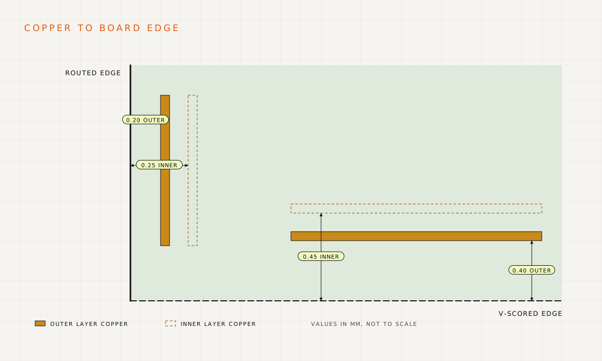
Plan view of a board corner showing a track and a pad near a routed edge and near a scored edge, with clearance callouts of 0.20 mm and 0.25 mm for routed edges and 0.40 mm and 0.45 mm for scored edges on outer and inner layers.
Copper clearance to the board edge depends on how the edge is made. Scoring needs more room than routing.

Drilling and vias

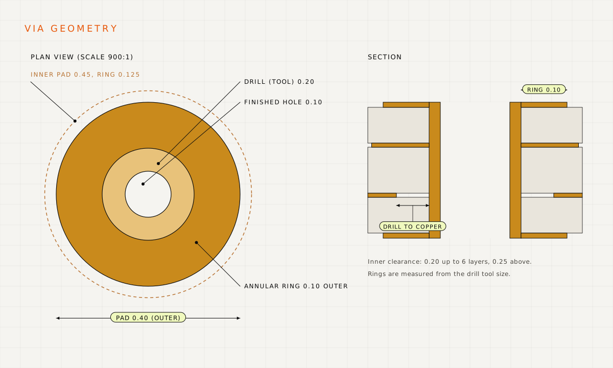
Plan and section view of a plated via: a 0.20 mm drill producing a 0.10 mm finished hole, a 0.40 mm outer pad leaving a 0.10 mm annular ring, a 0.45 mm inner pad with a 0.125 mm ring, and clearance from the drill to an inner-layer track.
Via geometry at our standard minimums. Rings are measured from the drill tool size, not the finished hole.
Drilling
ItemStandard capability
Smallest finished via hole0.10
Smallest via drill (tool size)0.20
Smallest via pad, outer layers0.40
Smallest via pad, inner layers0.45
Annular ring, outer layers (from tool size)0.10
Annular ring, inner layers (from tool size)0.125
Drill to drill (tool size)0.15
Smallest plated slot (tool size)0.50
Drill to inner-layer copper, up to 6 layers0.20
Drill to inner-layer copper, more than 6 layers0.25
Plated holes on the board edge: smallest drill0.60
Plated holes on the board edge: drill to drill0.20
Blind and buried vias
ItemStandard capability
Layer countUp to 24 layers, with up to 3 lamination (press) cycles
Extra press cyclesEach blind or buried span drilled after a lamination adds a press cycle; up to 3 in total
Smallest blind via0.20 drill, 0.10 finished, 0.125 annular ring
Largest blind via0.30 finished, keeping an aspect ratio of 1:8 or less
Drilling methodMechanical through-drilling of the sub-laminate; controlled-depth and laser drilling are not offered
Via fill
ItemStandard capability
Fill materialNon-conductive solder mask ink, suitable for vias near BGAs and in dense designs
Largest drill that can be filled0.35 (about 0.25 finished)

Surface finishes

Finishes and thicknesses
FinishThicknessRoHS
HASL, tin-lead1 to 25 µmNo
HASL, lead-freeBy quoteYes
Immersion tinBy quoteYes
ENIGNickel 3 to 6 µm; gold 0.04 µm minimum, typically 0.075 to 0.10 µmYes
Hard gold (electrolytic nickel gold)Nickel 3 to 6 µm; gold 0.5 µm minimumYes

Dielectrics and impedance

Layer construction
ItemStandard capability
Thinnest core0.10
Thinnest dielectric0.10
Controlled impedanceYes, with measurement on test coupons

Solder mask and legend

Solder mask
ItemGreen and blueOther colours
Mask opening (expansion per side)0.060.10
Smallest mask web between pads0.080.12
Mask opening to track0.100.10
Legend and colours
ItemStandard capability
Legend line width0.10 minimum
Legend character height1.00 minimum
Legend coloursWhite, black, yellow
Solder mask coloursGreen, blue, black, white, red, purple, yellow, orange

Profiling and edge clearance

Routing and scoring
ItemStandard capability
V-score angle30°
Jump scoringYes
Smallest router bit0.50
Copper to routed edge, outer layers0.20
Copper to routed edge, inner layers0.25
Copper to scored edge, outer layers0.40
Copper to scored edge, inner layers0.45

Carbon ink and peelable mask

Special processes
ItemStandard capability
Carbon ink
Smallest carbon line0.30
Smallest carbon to carbon gap0.25
Peelable solder mask
Narrowest peel-off element0.50
Largest hole covered (finished size)6.00
Mask overlap onto the copper pattern0.254 or more
Gap to exposed copper that stays uncovered0.254 or more
Gap to the board outline0.50 or more

Also available: impedance control, blind and buried vias, carbon contacts, hard gold edge tabs and peelable mask. Design rules for these layers are in the PCB design guidelines.

Tolerances

Hole tolerances
Hole sizePlated (PTH)Non-plated (NPTH)
0.50 to 3.50±0.10±0.10
Above 3.50±0.15±0.15
Other tolerances
ItemTolerance
Board outline±0.20 mm
Board thickness, up to 0.8 mm±20%
Board thickness, above 1.0 mm±10%
Track width and spacing±20%
Copper in plated holes0.020 mm (20 µm) minimum
Bow and twist1% maximum

Order size

Prototype and production quantities are both welcome. A single standard order covers up to the board areas below; larger volumes are split into scheduled deliveries or quoted separately.

Board area per order
OrderTwo-layer boardsMultilayer boards
Fabrication onlyUp to 10 m²Up to 8 m²
Fabrication and assemblyUp to 15 m²Up to 10 m²

Ready when your files are

Send your design for a quote

Upload your Gerber, drill and assembly files with the quantities you need. Our engineers check them against these guidelines and come back with a price, a schedule and any questions.