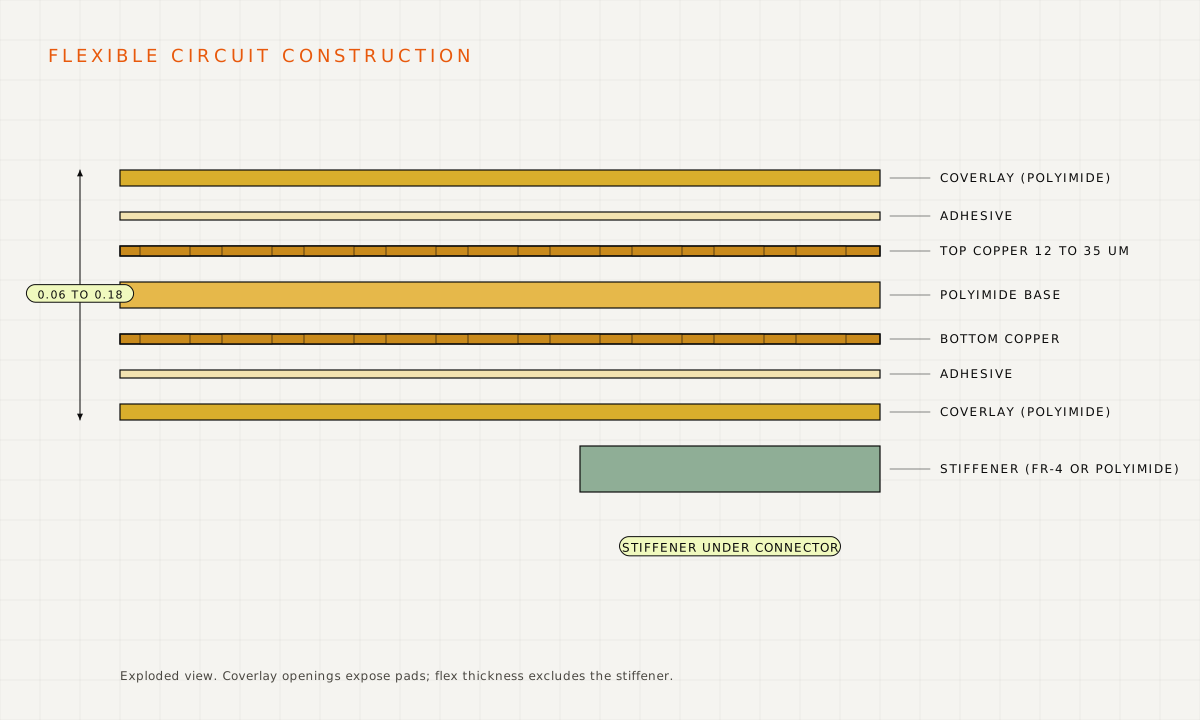
Our standard flexible circuits are one or two-layer polyimide constructions with coverlay, optional stiffeners and the finishes needed for connectors and soldered parts. Values are in millimetres unless stated.
A two-layer flexible circuit with coverlay on both sides and a stiffener behind the connector.
Circuit details
Item
Standard capability
Layers
1 or 2
Supplied as
Single circuits or in a panel you define
Largest circuit (L x W)
260 x 415
Finished thickness
0.06 to 0.18
Thickness tolerance
±0.05
Base material
Polyimide
Finished copper
12 µm to 35 µm (about 1/3 oz to 1 oz)
Tracks and drilling
Tracks, pads and holes
Item
Standard capability
Smallest track width
0.10
Smallest spacing
0.10
Smallest finished via (end diameter)
0.10
Smallest finished via pad
0.40
Smallest annular ring
0.10
Drill to drill
0.15
Smallest plated slot (tool size)
0.50
Smallest non-plated slot (tool size)
0.50
Countersinks (NPTH)
6.00, 6.50, 7.00 or 7.50 tool diameter
Hatched copper
Track 0.15, gap 0.15
Hole tolerances
Hole
Tolerance
Plated, below 3.5
±0.10
Plated, above 3.5
±0.15
Non-plated, below 3.0
±0.10
Non-plated, above 3.0
±0.15
Finishes and impedance
Surface finishes for flex
Finish
Nickel
Gold
Typical use
Electrolytic (hard) gold
3 to 5 µm
0.30 to 0.50 µm
Contact fingers and ZIF connector tails
ENIG
3 to 5 µm
0.05 to 0.075 µm
Soldered parts and flat pads
Immersion tin
None
None
Soldered parts at lower cost
Controlled impedance
Item
Standard capability
Impedance range
25 to 120 Ω, measured to your requirement
Coverlay, legend and stiffeners
Coverlay and legend
Item
Standard capability
Coverlay
Yellow polyimide coverlay: none, top, bottom or both sides
Legend colour
White
Legend line width
0.10 minimum
Legend character height
1.00 minimum
Serial numbers
Available on single circuits
Stiffeners
Item
Standard capability
Material
FR-4 or polyimide
Placement
None, top, bottom or both sides
Finish under stiffened areas
ENIG or immersion tin
Copper
12 µm or 35 µm
Profiling and special layers
Profile, carbon and peelable mask
Item
Standard capability
Copper to circuit edge, outer layers
0.20
Smallest router bit
0.50
Scoring
Not available for flex
Smallest carbon line
0.30
Smallest carbon to carbon gap
0.25
Narrowest peel-off element
0.50
Largest hole covered by peel-off
6.00
Peel-off overlap onto copper and clearance to free copper
0.254 minimum
Peel-off distance from outline
0.50 minimum
Designing for bending
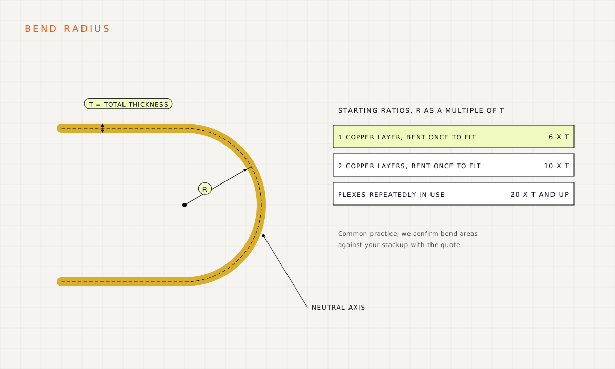
How tightly a circuit can bend depends on its total thickness, the number of copper layers and whether it bends once during installation or flexes in use. Common industry practice is a starting point; we review the bend areas on your drawing with the quote.
Bend radius is set as a multiple of total thickness. Dynamic flexing needs far more room than a one-time bend.
Run tracks at right angles to the bend line and keep them evenly spread across the width.
Keep vias, pads and stiffener edges out of the bend area.
On two-layer circuits, stagger top and bottom tracks rather than stacking them, so the copper does not form an I-beam.
Use rounded inside corners on the outline and slits to stop tears starting.
Use hatched copper instead of solid planes where a ground area has to bend.
Ready when your files are
Send your design for a quote
Upload your Gerber, drill and assembly files with the quantities you need. Our engineers check them against these guidelines and come back with a price, a schedule and any questions.